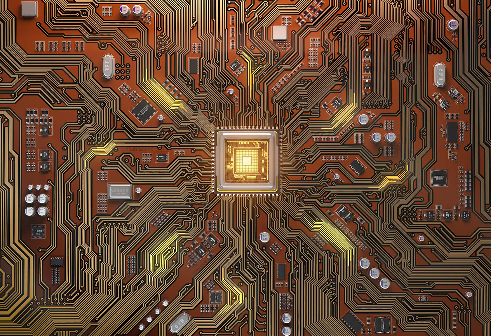
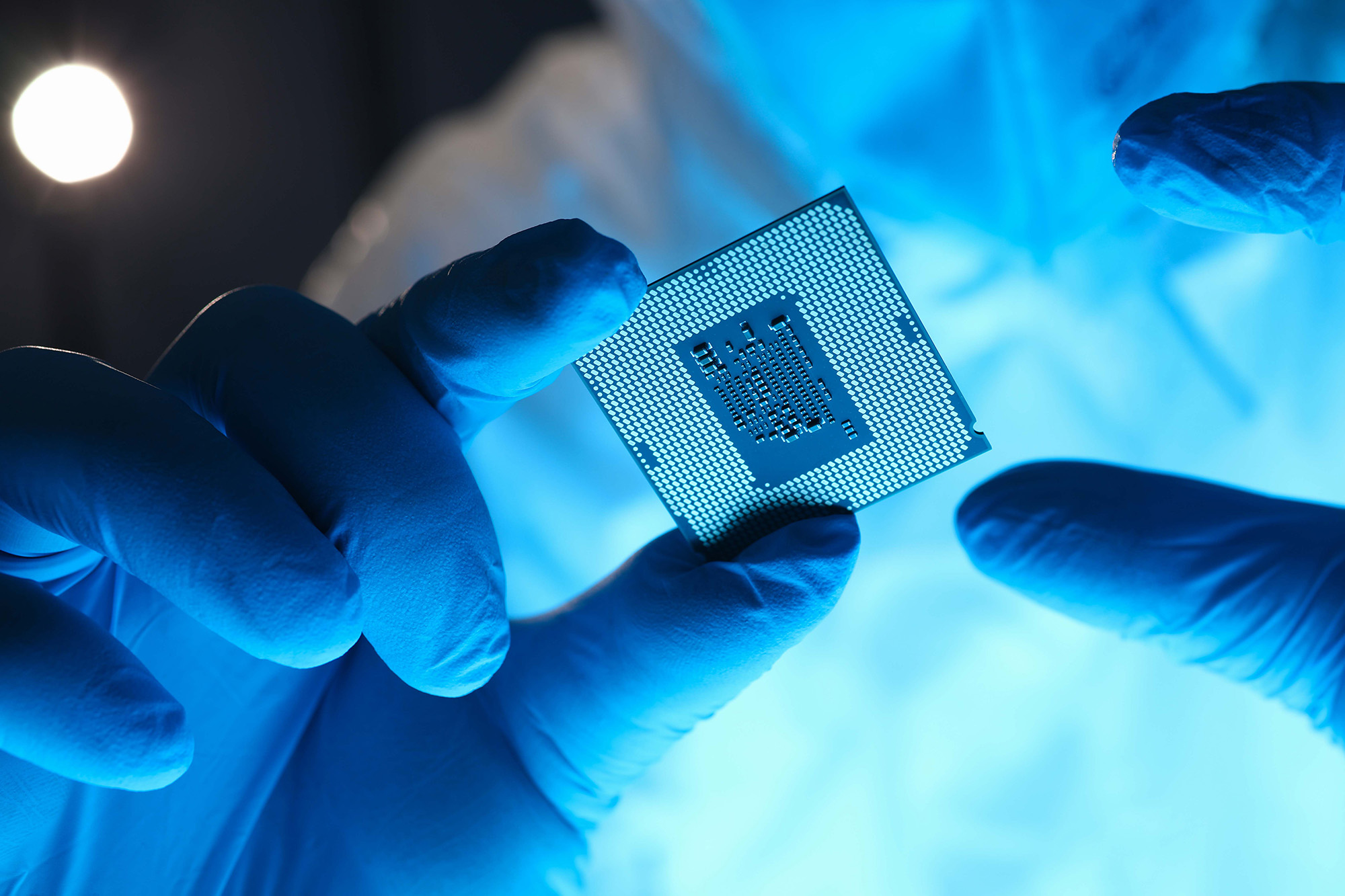
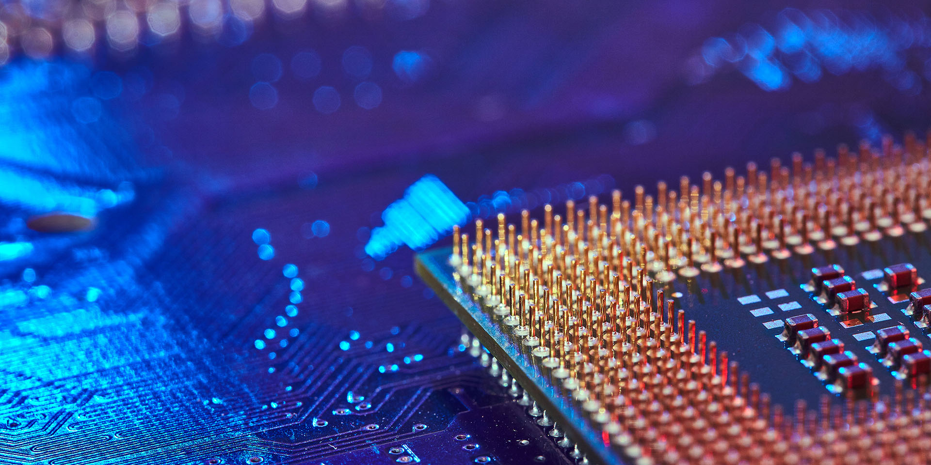
As we reach the limits of Moore’s Law using silicon chips, the challenges of energy demand, global supply, and climate change demand a new approach. We’re partnering with industry, universities, and national labs to develop new materials and techniques for smaller, faster, and more energy-efficient microelectronics.

Devices and complementary metal-oxide semiconductor (CMOS) technology
Exploring, identifying, modeling, and demonstrating new materials and devices to achieve ultra-efficient computing and increased performance.
Advanced manufacturing and integration
Leveraging our expertise in extreme ultraviolet (EUV) lithography and materials to develop novel nanomanufacturing methods to increase chip density.
Architecture
Applying our expertise in advanced computing to exploit new devices, materials systems, and packaging technologies developed in the first two thrusts.
Programming models
Creating new paradigms integrated with the new systems that define how application designers interact with the machine.
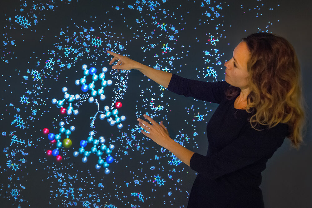
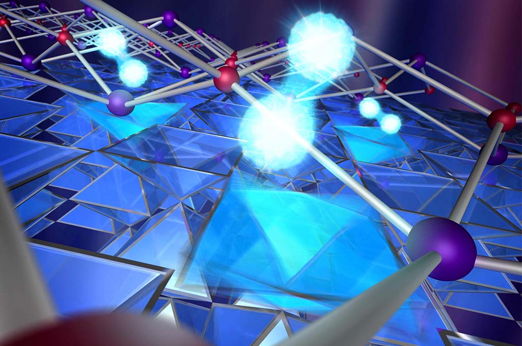
Quantum materials research and discovery
Developing and understanding new synthetic materials and their electronic, spin, chemical, and physical properties.
Center for X-ray Optics (CXRO)
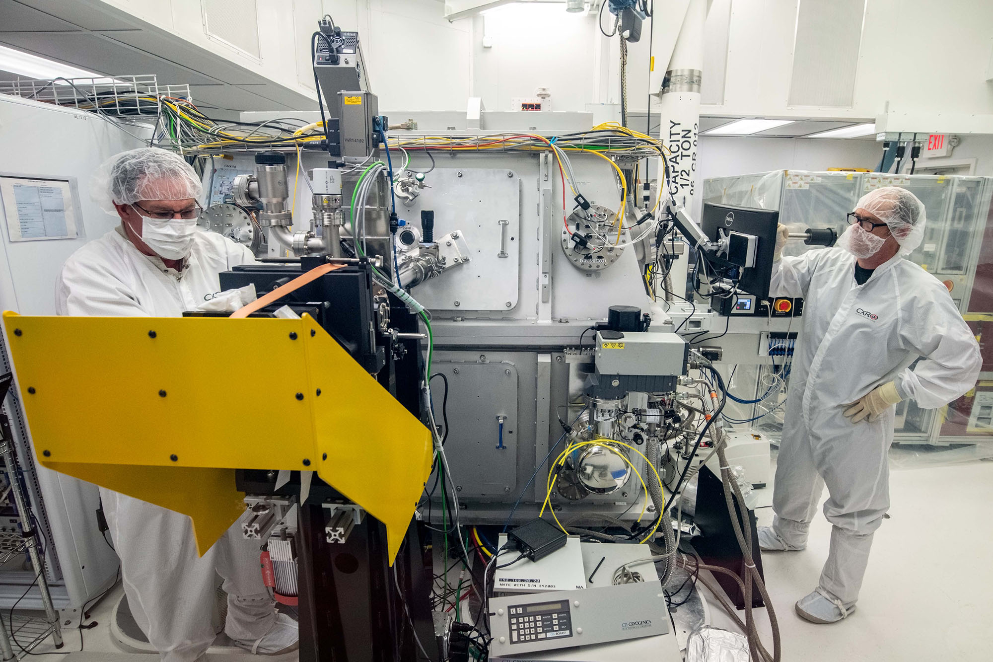
Developing EUV systems to address national needs in health, the environment, and semiconductor manufacturing.
Center for High Precision Patterning Science (CHiPPS)
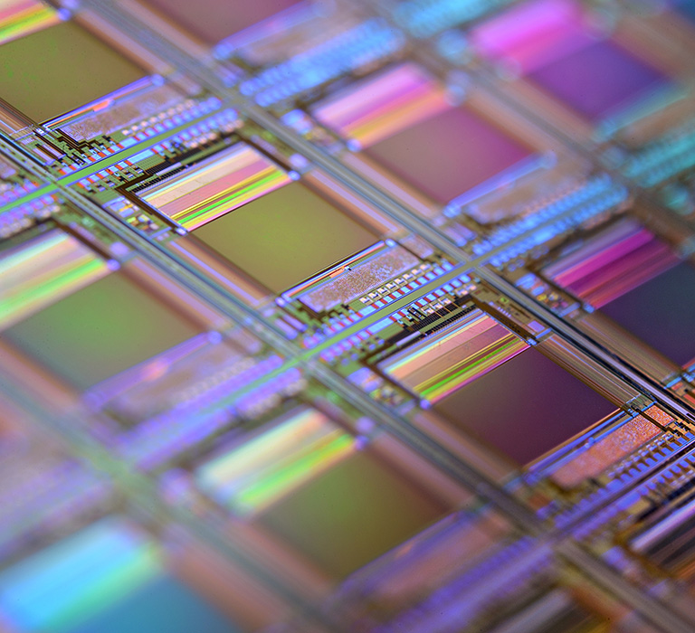
Creating a fundamental understanding and control of patterning processes for advanced manufacturing of future-generation microelectronics.
Co-design of Ultra-Low-Voltage Beyond CMOS Microelectronics

Exploring new physics leading to higher energy efficiency in computing.
Co-design and Integration of Nano-sensors on CMOS
Developing nano-material layers to add new capabilities to CMOS chips.
Microscopic and Electronic STRucture Observatory (MAESTRO) beamline

Dedicated to determining the electronic structure of materials at the mesoscopic (10–100 nm) scale.
Quantum Materials Program
Investigating how next-gen electronic materials respond to pulses of intense light.
Electronic Materials Program

Developing semiconductors of novel composition and morphology for energy applications.
Density Functional Theory Beyond Moore’s Law: Extreme Hardware Specialization for the Future of HPC
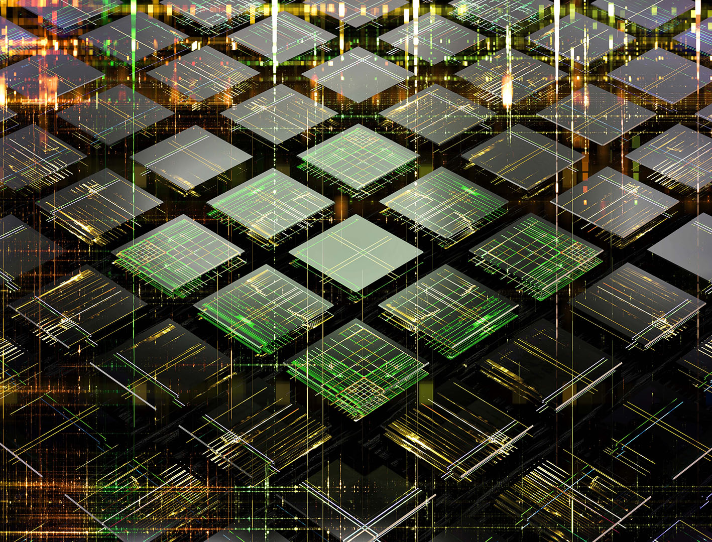
Illustrating the potential of purpose-built architectures as a potential future for high-performance computing applications.
Intelligence Advanced Research Projects Activity (iARPA) SuperTools
Developing tools to allow design and simulation of digital superconductor electronic circuits.
Photonically Interconnected data center Elements (PINE)
Developing an energy efficient, flexibly interconnected photonic data center architecture for extreme scalability.
Project 38

Developing a set of vendor-agnostic architectural explorations to quantify value to the Department of Energy (DOE) and Department of Defense.
Post Moore Architecture and Accelerator Design Space Exploration Using Device Level Simulation and Experiments (PARADISE)

An open-source comprehensive method to evaluate emerging technologies.
PARADISE++

Building a large-scale HPC framework to simulate post-Moore architectures built using emerging technologies.
Adaptive mesh Refinement Time-domain ElectrodynaMics Solver (ARTEMIS)
A full physical electromagnetic simulation framework for modeling next-generation microelectronics.
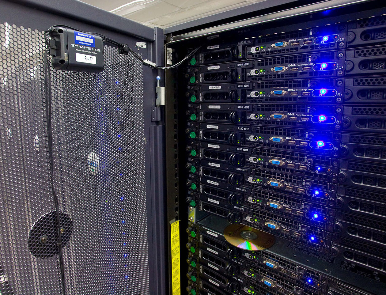
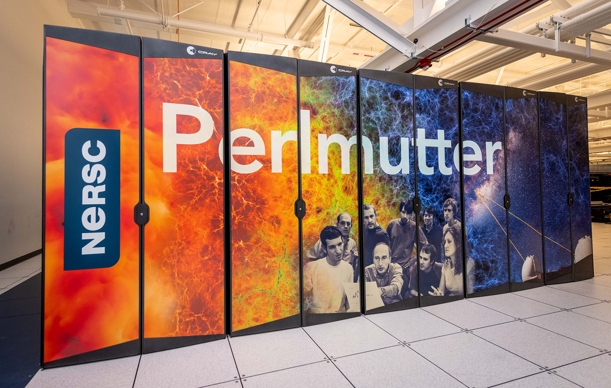
Advanced technologies research at the National Energy Research Scientific Computing Center (NERSC)
Enabling and supporting the development of next-generation HPC platforms and applications.
The Materials Project
Accelerating innovation in materials research for batteries, solar cells, and computer chips.
We foster strong partnerships that guide innovations from the Lab toward the marketplace. See our microelectronics technologies.

"The mission of the CHiPPS center is to create new fundamental understanding and control of patterning materials and processes with atomic precision. The goal is to enable the large-scale manufacturing of next-generation microelectronics."

"Our work shows that we need to go beyond the analogy of Lego blocks to understand devices made from stacks of disparate atomically-thin, two-dimensional materials. The seemingly distinct layers communicate through shared electronic pathways, allowing us to access and eventually design functionalities that are greater than the sum of the parts."

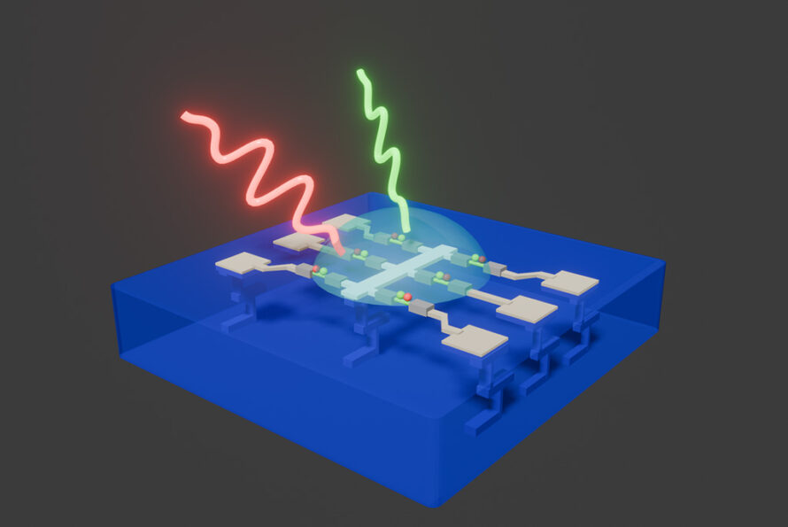
"We are interested in the topology of various photonic systems. We developed one of the first models that allow the understanding of the twist degree of freedom in moiré photonic structures and the prediction of novel optical properties in such systems."

A research team co-led by Berkeley Lab, Columbia University, and Universidad Autónoma de Madrid has developed a new optical computing material from photon avalanching nanoparticles. The breakthrough paves the way for fabricating optical memory and transistors on a nanometer size scale comparable to current microelectronics.
Berkeley Lab staff scientist Maurice Garcia-Sciveres is leading a collaboration with UC Berkeley and Sandia National Laboratories to develop powerful light-sensing microchips. The team is leveraging their expertise in nano-materials and integrated circuit design to develop new materials and techniques for smaller, faster, and more energy-efficient microelectronics that can be used to address societal challenges.
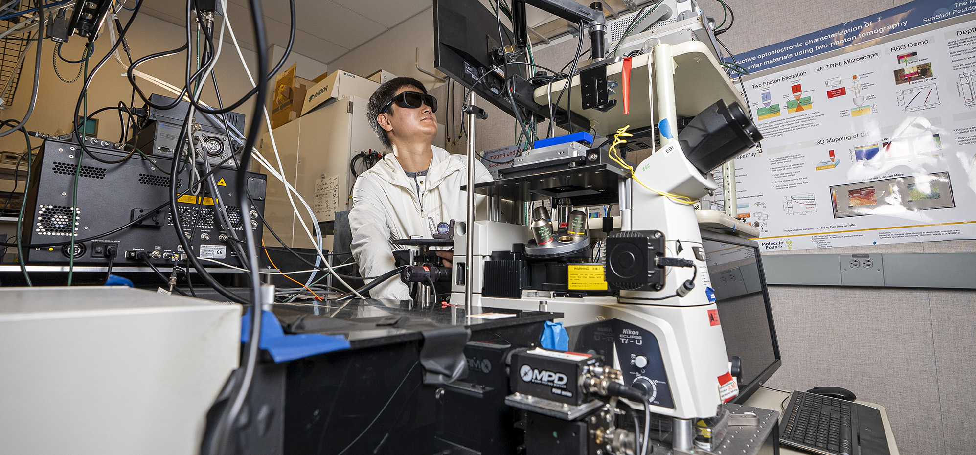
Berkeley Lab scientists are exploring ways to make energy-efficient microchips and push the boundaries of what’s possible in a world increasingly integrated with technology.
A New Approach to Efficient Optoelectronics, Inspired by the Human Eye
Scientists Capture Images of Electron Molecular Crystals

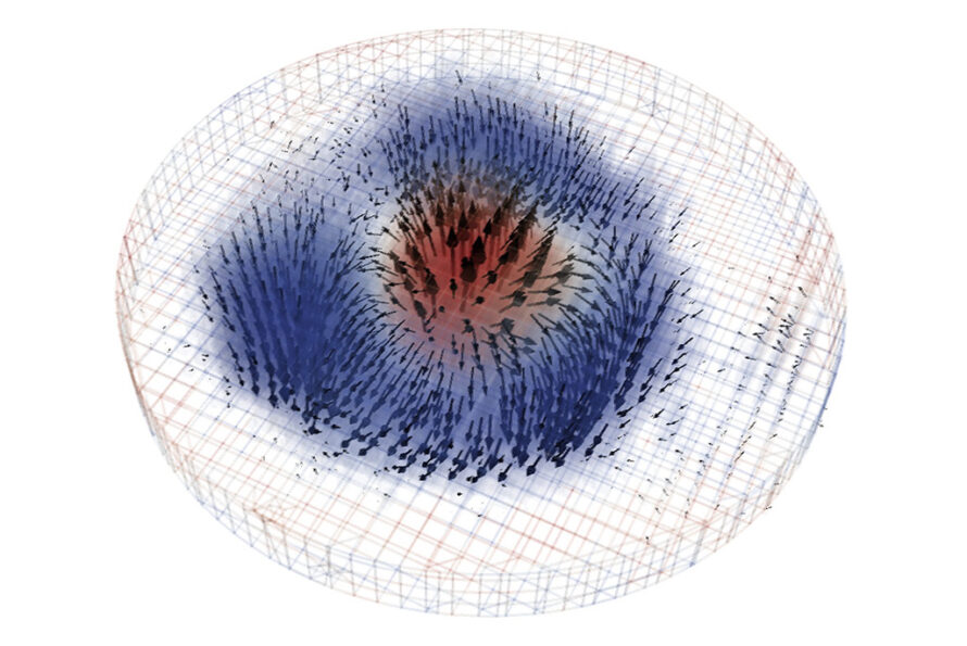
Researchers Succeed in Taking 3D X-ray Images of a Skyrmion
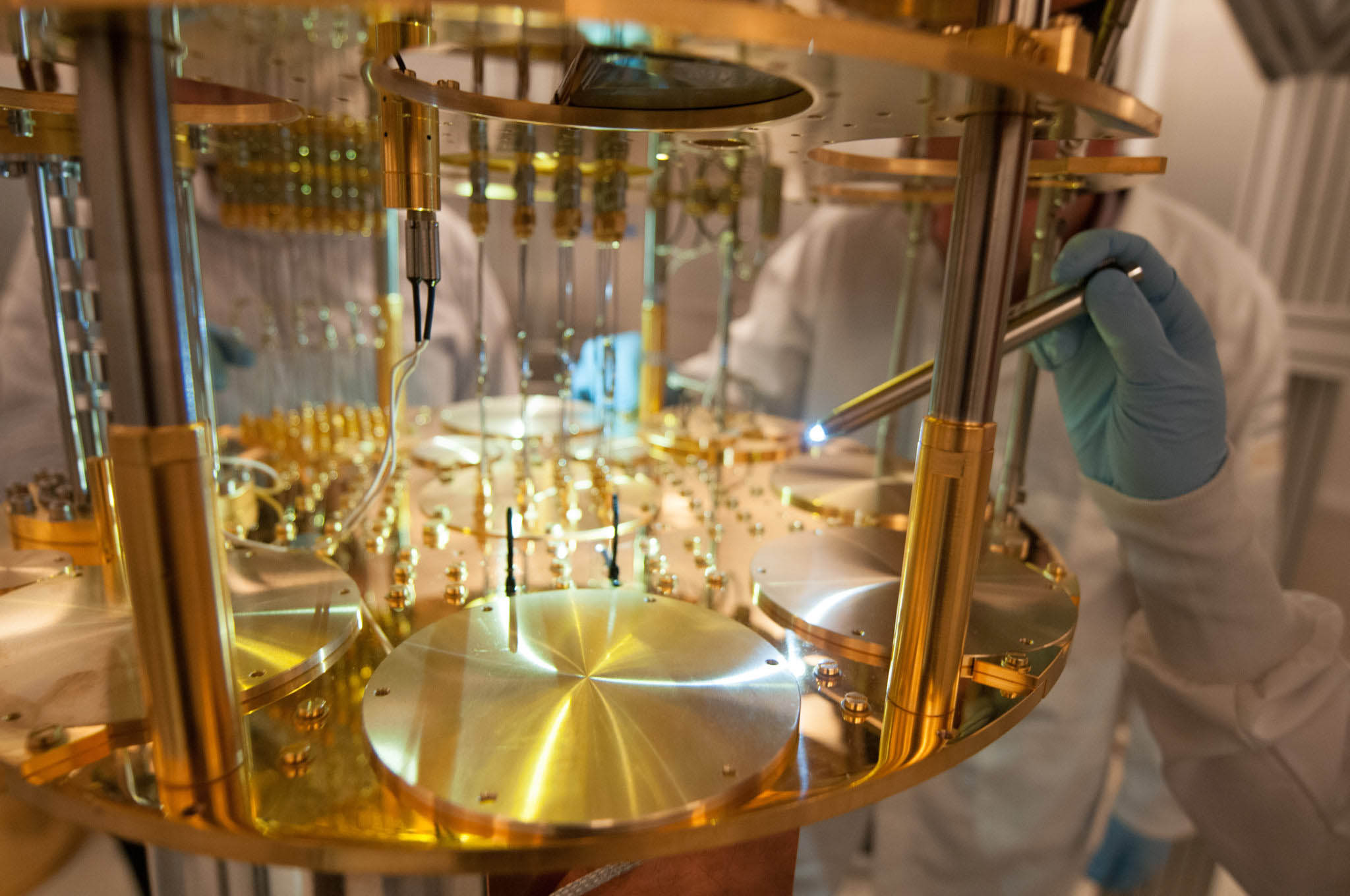
Quantum Science
Frontier Computer Sciences
Materials and Chemical Sciences